- 您现在的位置:买卖IC网 > Sheet目录507 > SI1046R-T1-E3 (Vishay Siliconix)MOSFET N-CH 20V 606MA SC75-3
Si1046R
Vishay Siliconix
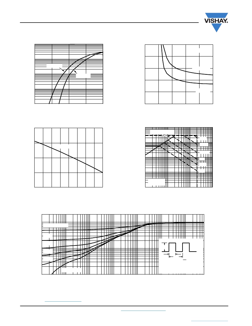
TYPICAL CHARACTERISTICS (T A = 25 °C, unless otherwise noted)
10
1.0
I D = 0.606 A
0. 8
1
0.1
0.01
0.001
T J = 150 °C
T J = 25 °C
0.6
0.4
0.2
0.0
T A = 125 °C
T A = 25 °C
0
0.3
0.6
0.9
1.2
0
1
2
3
4
5
1.0
V SD - So u rce-to-Drain V oltage ( V )
Source-Drain Diode Forward Voltage
10
V GS - Gate-to-So u rce V oltage ( V )
R DS(on) vs. V GS vs Temperature
Limited b y R DS(on) *
1 ms
0. 8
I D = 250 μ A
1
10 ms
100 ms
0.6
0.4
0.2
0.1
0.01
0.001
T A = 25 °C
Single P u lse
1s
10 s
DC
- 50
- 25
0
25
50
75
100
125
150
0.1
1
10
100
T J - Temperat u re (°C)
Threshold Voltage
V DS - Drain-to-So u rce V oltage ( V )
* V GS > minim u m V GS at w hich R DS(on) is specified
Safe Operating Area, Junction-to-Ambient
2
1
D u ty Cycle = 0.5
0.2
N otes:
0.1
0.1
0.05
P DM
t 1
t 1
0.01
0.02
Single P u lse
t 2
1. D u ty Cycle, D =
t 2
2. Per Unit Base = R thJA = 540 °C/ W
3. T JM - T A = P DM Z thJA(t)
4. S u rface Mo u nted
10 -4
10 -3
10 -2
10 -1
1
1 0
100
6 0 0
S qu are W a v e P u lse D u ration (s)
Normalized Thermal Transient Impedance, Junction-to-Ambient
Vishay Siliconix maintains worldwide manufacturing capability. Products may be manufactured at one of several qualified locations. Reliability data for Silicon
Technology and Package Reliability represent a composite of all qualified locations. For related documents such as package/tape drawings, part marking, and
reliability data, see www.vishay.com/ppg?74595 .
www.vishay.com
4
For technical questions, contact: pmostechsupport@vishay.com
Document Number: 74595
S13-0195-Rev. D, 28-Jan-13
This document is subject to change without notice.
THE PRODUCTS DESCRIBED HEREIN AND THIS DOCUMENT ARE SUBJECT TO SPECIFIC DISCLAIMERS, SET FORTH AT www.vishay.com/doc?91000
发布紧急采购,3分钟左右您将得到回复。
相关PDF资料
SI1046X-T1-GE3
MOSFET N-CH 20V 606MA SC89-3
SI1050X-T1-GE3
MOSFET N-CH D-S 8V SC-89-6
SI1051X-T1-E3
MOSFET P-CH 8V 1.2A SC89-6
SI1056X-T1-GE3
MOSFET N-CH D-S 20V SC-89-6
SI1058X-T1-GE3
MOSFET N-CH 20V SC89
SI1065X-T1-GE3
MOSFET P-CH 12V 1.18A SC89-6
SI1067X-T1-GE3
MOSFET P-CH 20V 1.06A SC89-6
SI1070X-T1-GE3
MOSFET N-CH 30V 1.2A SOT563F
相关代理商/技术参数
SI1046RT1GE3
制造商:Vishay Angstrohm 功能描述:Trans MOSFET N-CH 20V 0.606A 3-Pin SC-75 T/R
SI1046R-T1-GE3
功能描述:MOSFET 20V 606mA 0.25W 420mohm @ 4.5V RoHS:否 制造商:STMicroelectronics 晶体管极性:N-Channel 汲极/源极击穿电压:650 V 闸/源击穿电压:25 V 漏极连续电流:130 A 电阻汲极/源极 RDS(导通):0.014 Ohms 配置:Single 最大工作温度: 安装风格:Through Hole 封装 / 箱体:Max247 封装:Tube
SI1046X
制造商:VISHAY 制造商全称:Vishay Siliconix 功能描述:N-Channel 20-V (D-S) MOSFET
SI1046X-T1-E3
功能描述:MOSFET 20V 0.606A 0.25W RoHS:否 制造商:STMicroelectronics 晶体管极性:N-Channel 汲极/源极击穿电压:650 V 闸/源击穿电压:25 V 漏极连续电流:130 A 电阻汲极/源极 RDS(导通):0.014 Ohms 配置:Single 最大工作温度: 安装风格:Through Hole 封装 / 箱体:Max247 封装:Tube
SI1046X-T1-GE3
功能描述:MOSFET 20V 606mA 0.25W 420mohm @ 4.5V RoHS:否 制造商:STMicroelectronics 晶体管极性:N-Channel 汲极/源极击穿电压:650 V 闸/源击穿电压:25 V 漏极连续电流:130 A 电阻汲极/源极 RDS(导通):0.014 Ohms 配置:Single 最大工作温度: 安装风格:Through Hole 封装 / 箱体:Max247 封装:Tube
SI104-820
制造商:未知厂家 制造商全称:未知厂家 功能描述:SMT Power Inductor
SI104-820K
制造商:DELTA 制造商全称:Delta Electronics, Inc. 功能描述:SMT Power Inductor
SI1050X
制造商:VISHAY 制造商全称:Vishay Siliconix 功能描述:N-Channel 8-V (D-S) MOSFET
